MIOS:
IBM 5150 BIOS Replacement
Project
by
M. Mruzek for MTM Scientific, Inc
This
webpage describes the MIOS Project. MIOS is a
chip-for-chip replacement of the BIOS (Basic Input Output System) on
the IBM 5150 Personal Computer. On the IBM PC the BIOS is contained in
a ROM IC Chip located on the motherboard at socket location U33. The IC
is socketed and can be replaced with a custom ROM containing
custom code.
The purpose of this project is to explore controlling the IBM PC
hardware in non-standard ways. The purpose is not to replace the BIOS
with another BIOS that does exactly the same thing! We are going to
describe how MIOS works by describing the path we took for development.
We started this project by considering other BIOS replacement software.
Notably for the IBM PC there is a diagnostic ROM replacement known as
the Landmark/Supersoft package, as described here: Minus
Zero Degrees
The Landmark/Supersoft code is unique. By burning the code
to ROM and placing in BIOS location U33 it is possible to boot the IBM
PC and perform a series of diagnostic tests, with the results
reported on the screen in real time. A photo of a typical display
screen is shown in Figure 1. The
key point about the
diagnostic
ROM is the fact the code is completely controlling the PC
hardware: There is no DOS operating system. There is no BIOS.
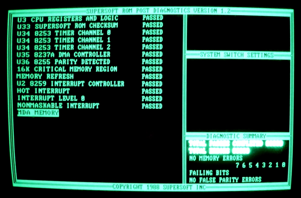 Figure
1: Landmark / Supersoft Diagnostic ROM Display
Figure
1: Landmark / Supersoft Diagnostic ROM Display
Controlling PC hardware directly, without using the standard BIOS, is
facilitated by the extensive available documentation describing
how the IBM 5150
works and operates. The IBM Technical Manual contains the complete
circuit diagrams, with useful additional descriptions of hardware
components, and a complete listing of the BIOS source code. The
assembly code control of computer hardware without a BIOS
or operating system is sometimes referred to as using "primitives".
Direct control of computer hardware has certain advantages, not the
least of
which is the possibly of increased operating speed.
As built, the IBM 5150 PC dedicated a single ROM socket for the BIOS.
This is socket U33 on the motherboard, as shown in Figure 2. The socket
is designed to accept
a Motorola MC68766 programmable ROM. The ROM has space for
8192
bytes of code. (This is often abbreviated as "8K".) The original ROM
chip chosen by IBM is comparatively rare, and the programming protocol
requires vintage hardware that can be difficult to find.
Fortunately, the ROM chip can be substituted with a much more common IC
chip by using a socket adapter. The MIOS code must be burned into a ROM
chip before it can be used. We use an adapter with the
programmable M27128A
chip,
as shown in Figure 3.
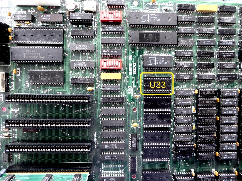 Figure
2: IBM 5150 PC BIOS socket location U33.
Figure
2: IBM 5150 PC BIOS socket location U33.
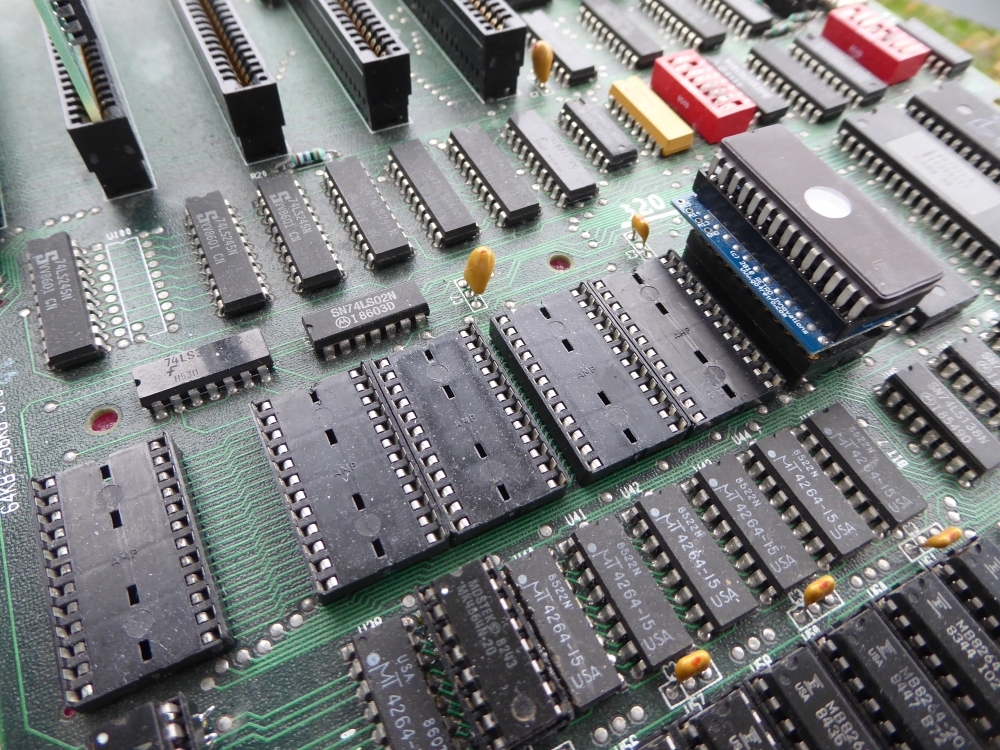 Figure
3: ROM Socket Adapter in U33.
Figure
3: ROM Socket Adapter in U33.
The maskable interrupts can be masked by using the assembly code
command "CLI", a mneumonic with the meaning "CLear Interrupts". As luck
would have it, the IBM 5150 external non-maskable interrupts can indeed
by
disabled with a command to a logic gate preceding the CPU input pin, as
described in Mazidi, P. 435. (Masking NMI
Interrupts) The internal non-maskable interrupts are
the only remaining. (Interrupt 0: Divide by
Zero, etc)
The 8088 CPU is
coded
internally to proceed to a specific memory address at the start of the
RAM to read an interrupt vector address to follow and execute code to
handle the interrupt. The first 16K of RAM in the IBM PC is soldered
directly to the motherboard. Although this RAM is available for use,
since it is dynamic RAM, the memory requires constant refreshing to
hold address byte content. Therefore we do not have an easy way to
handle the non-maskable internal CPU interrupts. We recognize this as a
deficiency in MIOS. Here is a discussion of operating without DRAM
refresh interrupts. (DRAM
Refresh)
MIOS is designed to operate in conjunction with an MDA display adapter.
The MDA is the simplest display adapter for the IBM 5150 PC. However,
the MDA
display adapter has one very notable and useful feature: The video
memory is SRAM, not RAM. The SRAM on the MDA card can be used
by
MIOS as general-purpose memory for creating a Stack Segment (SS) and
Extra Segment (ES). Using SRAM avoids the complexity and resource
requirements of servicing an interrupt for memory refresh.
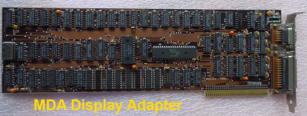 Figure
4: IBM Monochrome Display Adapter "MDA"
Figure
4: IBM Monochrome Display Adapter "MDA"
Before the MDA display adapter can be used it must be initialized. The
MDA is initialized by sending setup byte parameters to onboard memory
locations called registers. This
turns out to be fairly easy to do because of excellent documention
regards the inner workings of the MDA: MDA
Card Explanation
We were fortunate to also find a coding example for initializing the
MDA registers using assembly code. Although we did not use the code
directly, the basic outline in MIOS is very similar. MDA
Card
Initializaton Example
Working with the ROM code space of 8192 bytes is accomplished
by
using specialized software called a Hex Editor. It is akin to a text
editor, but optimized for editing hexadecimal machine code
instructions. Our favorite hex editor is HxD by Mael Horz, available
here: HxD
Hex Editor
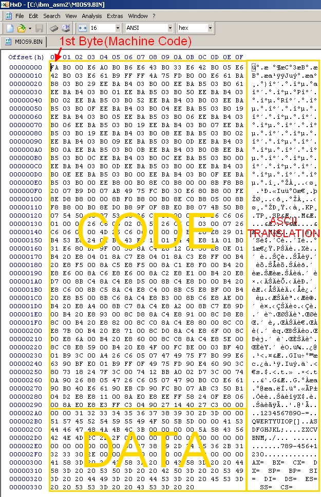 Figure
5: HxD Hex Editor review of a MIOS binary file
Figure
5: HxD Hex Editor review of a MIOS binary file
With a hex editor you can directly view and manipulate the 8192 bytes
of code for the MIOS ROM. A typical screenshot of a hex editing session
is shown in the Figure 5. The ROM space at motherboard location U33 is
hardwired to map to the 8088 memory space as locations FE00:0000 to
FF00:FFFF. (These addresses are represented in characteristic
Segment:Offset notation. See an explanation at Segment:Offset
Explanation) This memory is at
the very top of the
directly-addressable memory in the IBM 5150 PC.
The MIOS input/output operating system is coded in 8086 assembly code.
We have opted to code and compile using a software tool characteristic
of the time period. We are using Microsoft Assembler 2.0 ("MASM 2.0").
We use MASM to compile and link the code, and the "EXE2BIN.EXE utility
to "flatten" the executable to a simple binary file. (Basically to
remove the Program Segment Prefix (PSP).) Here is a link to historical
information for MASM: MASM
Version History
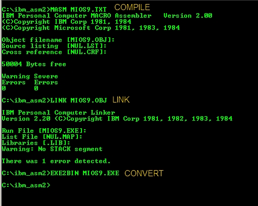 Figure
6: MASM 2.0 Compile, Link and EXE2BIN Conversion.
Figure
6: MASM 2.0 Compile, Link and EXE2BIN Conversion.
When power is applied, the 8088 CPU is internally programmed to
jump
to a specific memory location for its first machine code instruction.
That first instruction is expected to reside at memory location:
FF00:FFF0. This address corresponds to the beginning of the last 16
byte line in the U33 memory space. In the original IBM BIOS this
location contains an unconditional jump to the start of the boot code.
MIOS does the same thing, with an unconditional jump to the
first byte of the ROM at: FE00:0000.
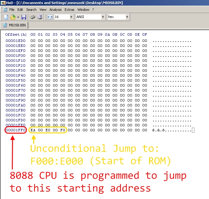 Figure
7: Unconditional Jump at CPU Cold Start
Figure
7: Unconditional Jump at CPU Cold Start
CS: Code Segment is a sequential list of machine code instructions for
the CPU.
DS: Data Space is a section of byte-based data the CPU can reference.
SS: Stack Segment is a temporary memory storage area, acessed using
PUSH and POP instructions.
ES: Extra Segment is a destination area for displaying
information, often the video monitor.
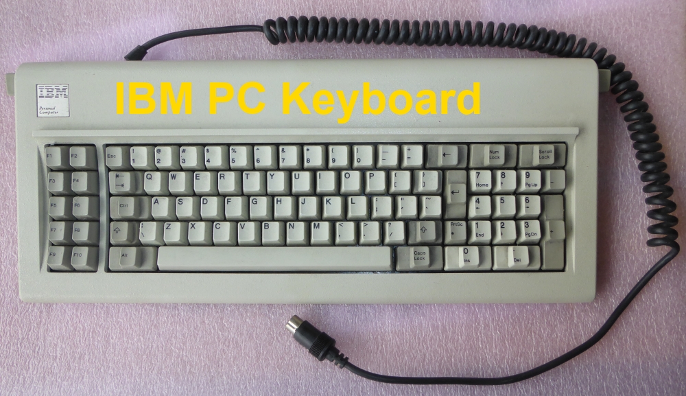
MIOS is written to interface directly with the IBM PC Keyboard. The
keyboard connects to the motherboard using a 5 Pin DIN connector. We
found a good assembly code example of a keyboard hardware interface in
Sam's Photofact Book: Keyboard Programming
Example The interface routine we are
using for the keyboard is extremely basic. The keyboard sends
byte-sized scancodes, which are different that the byte-sized ASCII
codes representing a character. A translation must be performed. We do
the translation using the XLAT instruction with a data table. (XLAT =
TRANSLATE). Another complication is that the keyboard actually sends 2
scancodes per key tap: 1 scancode for press, and 1 scancode for
release. The keyboard is polled for a keypress. Interrupts are not used.
 Figure
8: 83 Key IBM PC Keyboard
Figure
8: 83 Key IBM PC Keyboard
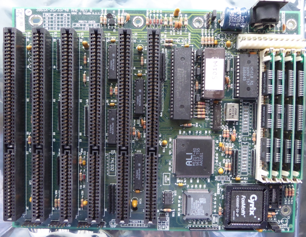
As an experiment, we created a 64K version of MIOS for a 386
motherboard as shown in Figure X. Because the motherboard has ISA
expansion slots, we were able to use the MDA video card. We were
surprised to discover that MIOS was able to boot the system. (Although
the keyboard interface did not work.) This experiment suggests
additional possibilities for future development.
We have packaged the source code and binary files for MIOS in a
compressed zip file. The file can be downloaded here: MIOS.ZIP
Here is an short summary of the sequential steps taken in the MIOS code:
1) Unconditional jump to the first byte in the U33 ROM memory space.
2) Mask and disable interrupts.
3) Beep the speaker
4) Initialize the MDA card
5) Clear the screen
6) Send a POST code to show boot progress (Requires
POST card at 80H
Port)
7) Define Data Segment, Extra Segment, Stack Segment
8) Display a welcome message ("MTM SCI")
9) Display a label in the Stack Segment ("STK")
10) Display 8088 CPU Registers
11) Poll the keyboard and display the ASCII character if a key is
pressed
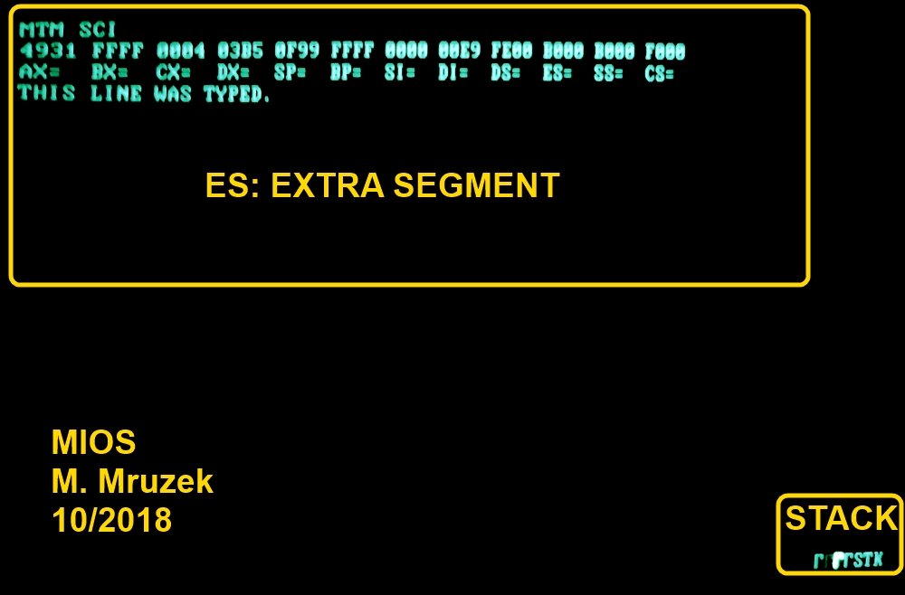 Figure
9: MIOS Welcome Screen
Figure
9: MIOS Welcome Screen
Here is a list of possible ideas for future improvements:
1) Programmed output on the parallet port on the MDA card. (Speed Test Results)
2) Use the DIP switch settings for input or configuration.
3) Program one of the onboard timers to measure short program
intervals. (Cycle Counter)
4) Add additional SRAM memory using an ISA card interface. (PC
SRAM Extension: SERGEY)
5) Create a dumb terminal using RS-232 I/O. (Serial
Port Card and the Initialize Code)
6) Add more features to the diagnostic interface. (Something like DEBUG)
7) Interface to a RTC card in an ISA slot. Poll the RTC registers for
timekeeping.
8) Interface to an 8087 FPU (Math Coprocessor)
9) Add hardware tests and diagnostics, with a progress display
10) Interface to CGA Video. Explore initializing a VGA card using the
registers.
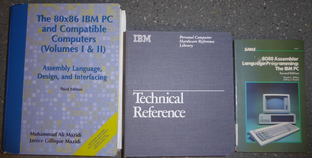
We consulted a large number of books and references developing the MIOS
code. Especially useful were the following books. The book by Mazidi
was especially helpful, and can be found on EBAY for less than $10.