|
Primary
Logic Family |
74LS
(Low-Power Schottky) |
|
Clock
Speed |
1 MHZ |
|
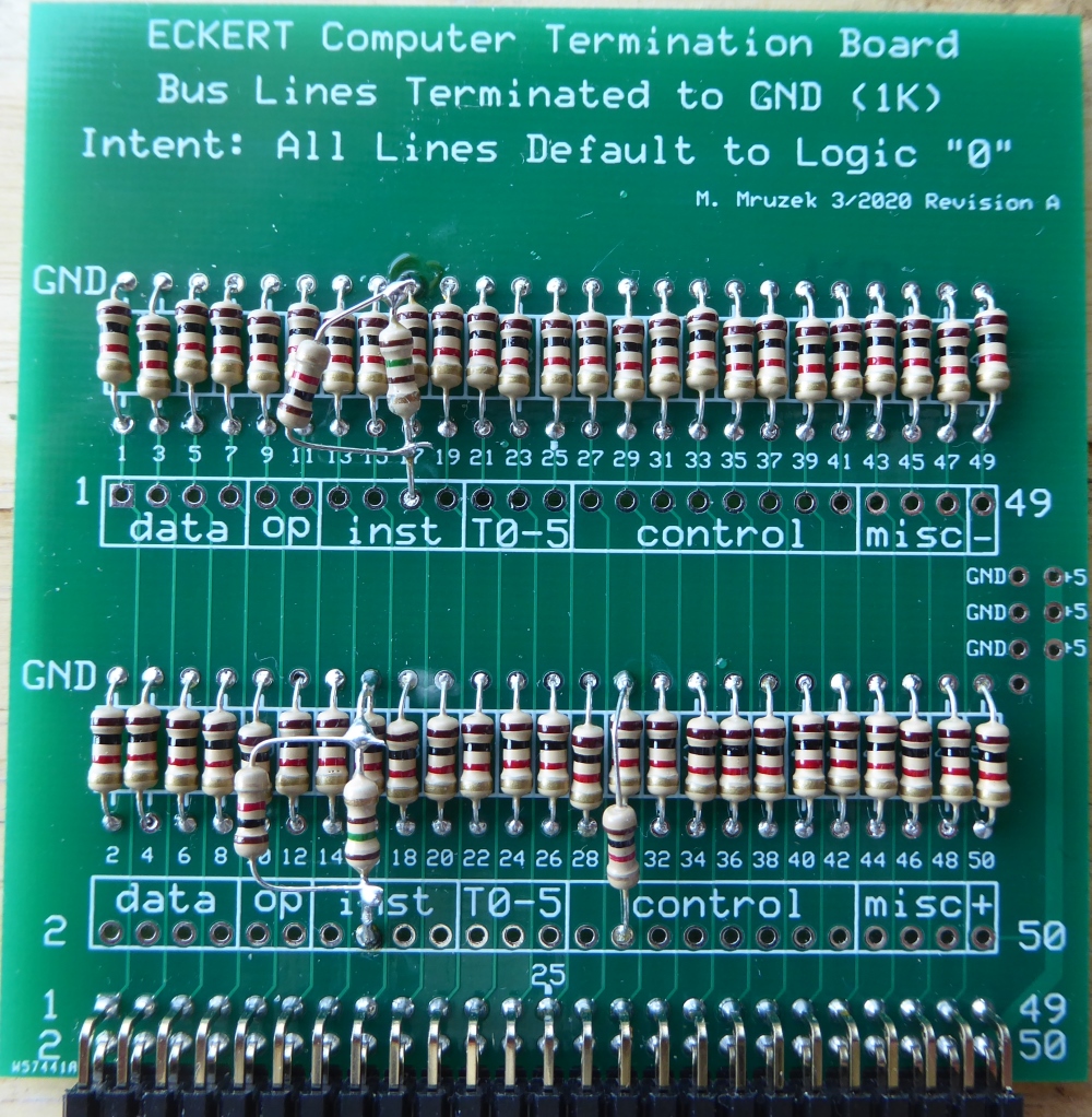
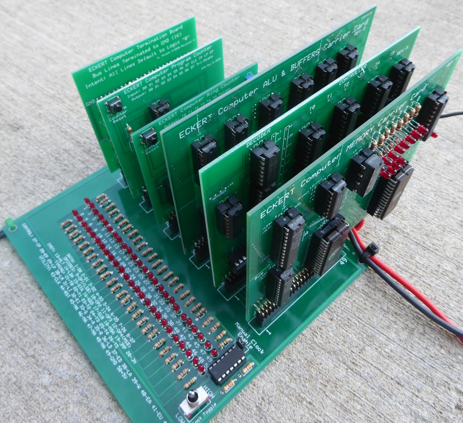
Bus
Architecture |
50
pin (“TTL-50” Bus) |
|
Data
Width |
12
bits |
|
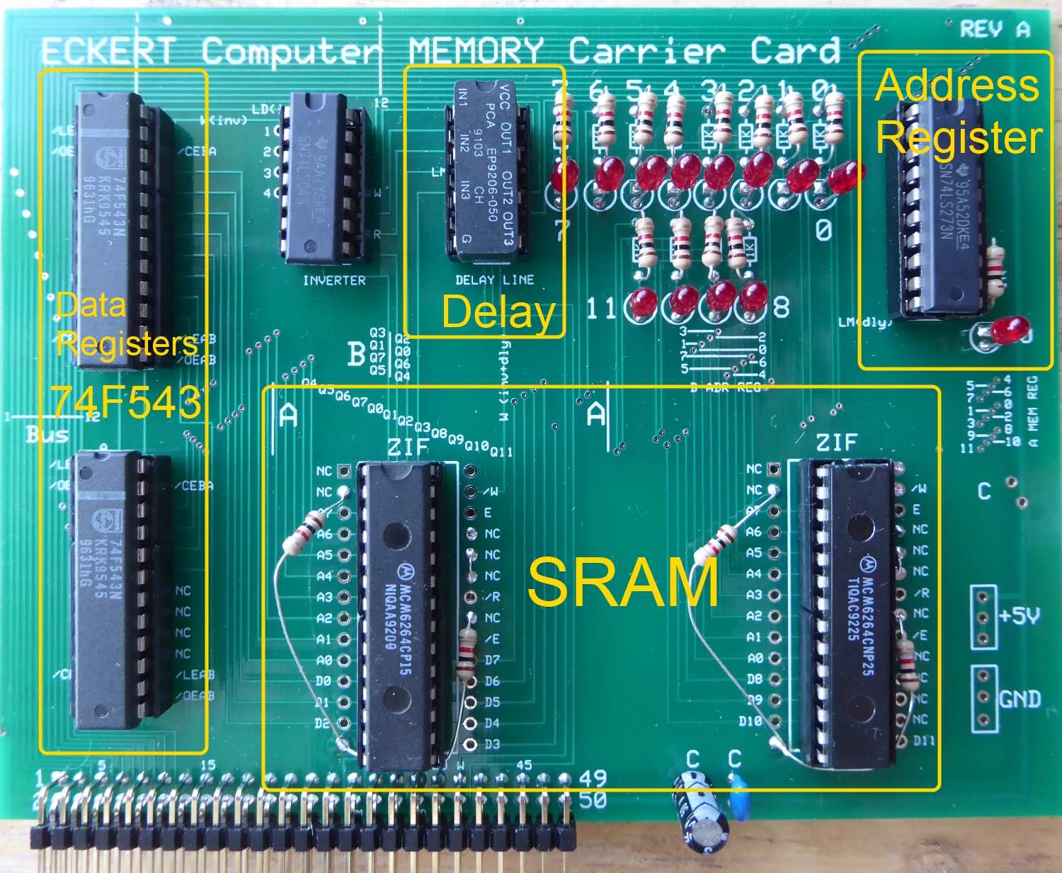
Memory
(ROM & SRAM) |
64K
(256 x 256, Equally Divided) |
|
Controller
Instructions |
16 |
|
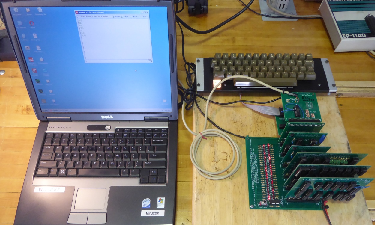
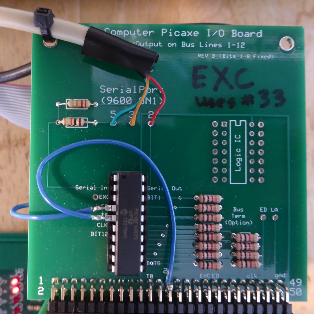
Keyboard |
Apple
II (with Parallel Output) |
|
Display |
40x2
LCD Module (4002) |
|
Hardware
Stacks |
3
(Keyboard, Data & Return) |
|
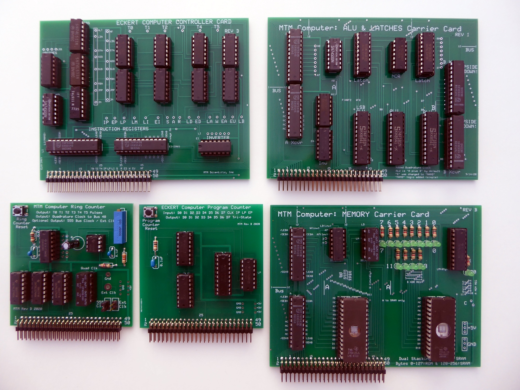
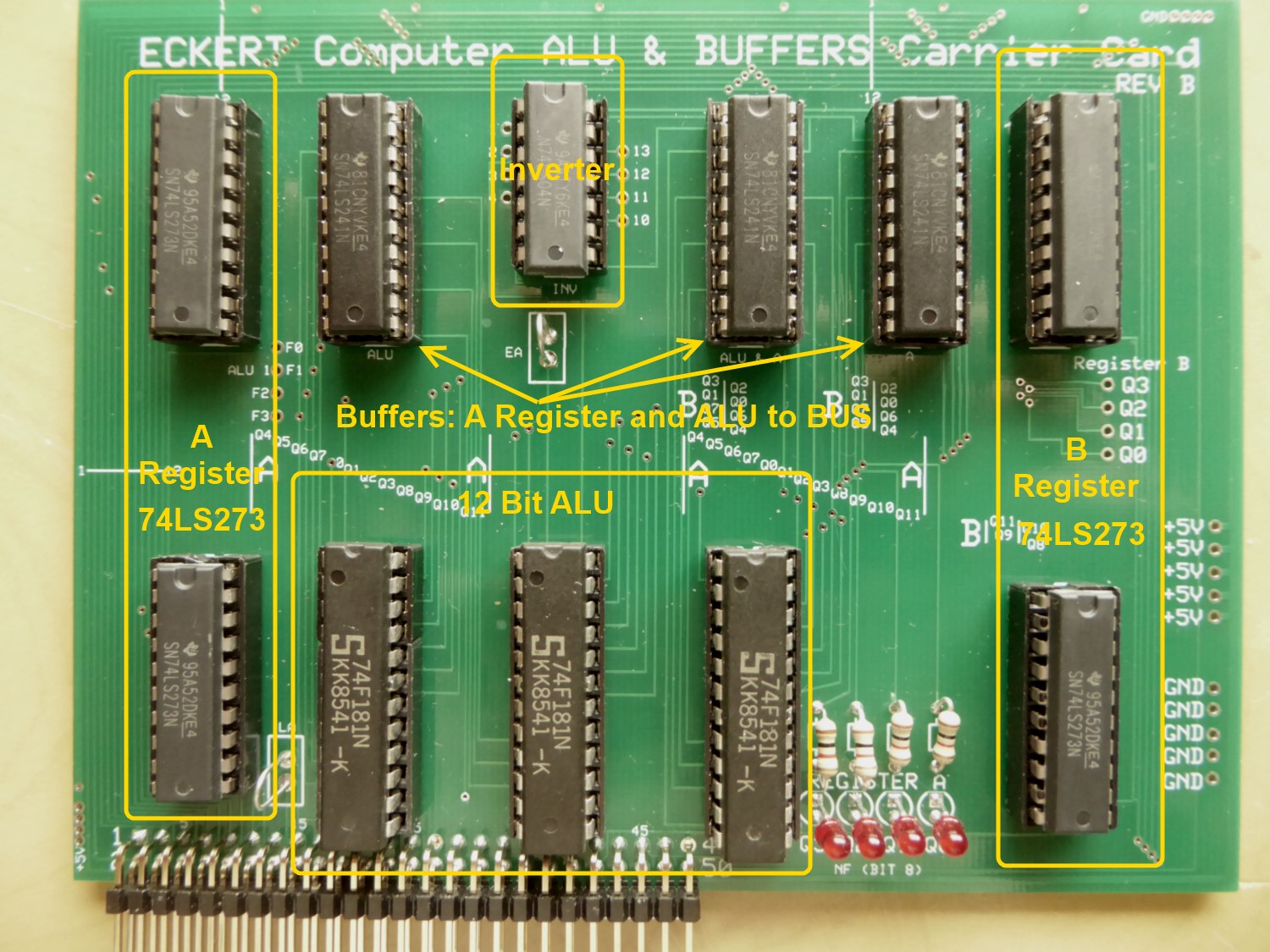
Arithmetic
Logic Unit |
74F181
(4 Bit Slice ALU, 3X) |
|
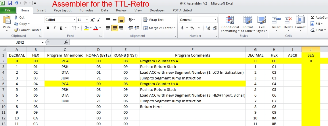
Assembler |
Custom
Excel Spreadsheet |
|
Programming
Language |
Threaded
Interpretive Language |
|
Hex
Code |
Mnemonic |
Description |
|
0 |
DTA |
Direct
To ACC (Immediate) |
|
1 |
RCL |
Recall
from Memory |
|
2 |
STO |
Store
to Memory |
|
3 |
ALU |
Arithmetic
Logic Unit Ops |
|
4 |
JLA |
Jump
Loading from ACC |
|
5 |
MAB |
Move
A to B |
|
6 |
JUM |
Jump
(Unconditional) |
|
7 |
JWE |
Jump
When Equal (A=B) |
|
8 |
PCA |
Program
Counter to ACC |
|
9 |
PSH |
Push
ACC to Stack |
|
A |
POP |
Pop
to ACC from Stack |
|
B |
INA |
In to
ACC from Bus |
|
C |
OUT |
Out
from ACC to Bus |
|
D |
JWG |
Jump
When Greater (A>B) |
|
E |
JWM |
Jump
When ACC Minus |
|
F |
CTR |
Counter
(Inc or Dec Stack) |
| Mnemonic | Description |
| LAZ | Load A with Zero |
| INC | Increment A |
| MAB | Move A to B |
| ADD | Add A and B |
| OUT | OUT A to Bus |
| POP | POP from Stack |
| PSH | PUSH to Stack |
| ASL | Arithmetic Shift Left |
| DEC | Decrement A |
| JLA | Jump Loading A |
| INA | IN A from Bus |
| NOP | No Operation |
| NAN | NAND of A with B |
| XOR | XOR of A with B |
| AND | AND of A with B |
| ORR | OR of A with B |
| MBB | Move B back to A |
| NTA | NOT A |
| NTB | NOT B (Result to A) |
| SUB | Subtraction A-B |
| SEG | Segment Memory Jump |
| PCA | Program Counter to A |
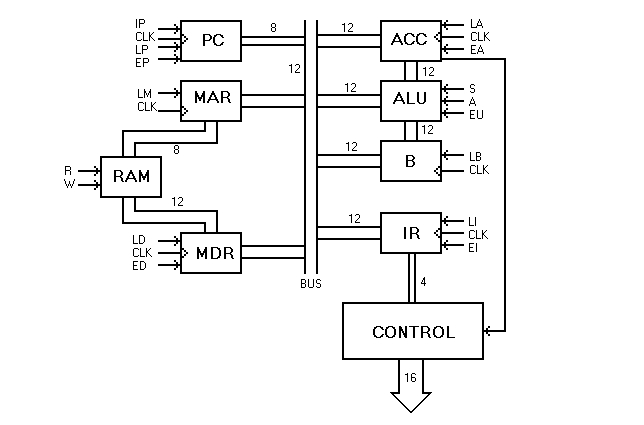
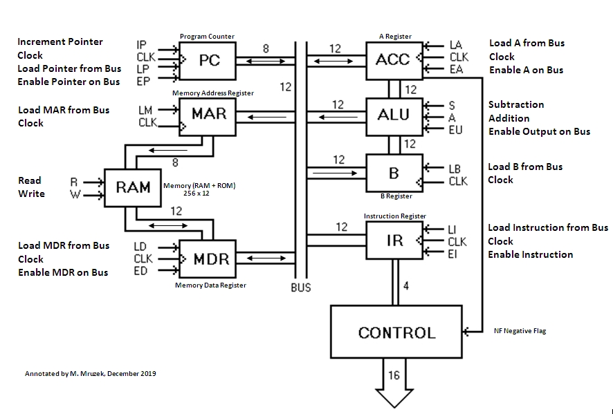
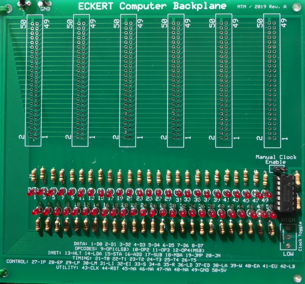
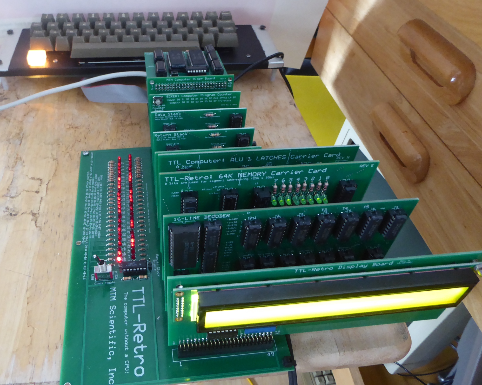
TTL-50 Bus
Assigments for the TTL-Retro
1
Data
0 (LSB), Also latched and sent as Bus #13 for microcode control of
hardware
2
Data
1, Also latched and sent on Bus as #14 for microcode control of hardware
3
Data
2, Also latched and sent on Bus as #15 for microcode control of hardware
4
Data
3, Also latched and sent on Bus as #16 for microcode control of hardware
5
Data
4, Also latched and sent on Bus as #17 for microcode control of hardware
6
Data
5, Also latched and sent on Bus as #18 for microcode control of hardware
7
Data
6, Also latched but not sent on Bus (No room on Bus)
8
Data
7, Also latched but not sent on Bus (No room on Bus)
9
OP1
(LSB) Instruction Bit, or Data 8
10
OP2 Instruction Bit, or Data 9
11
OP3 Instruction Bit, or Data 10
12
OP4 (MSB) Instruction Bit, or Data 11
13
Microcode: CN (ALU*), or Decrement Selected Stack, or I/O
Device Selection (Latched Bus #1)
14
Microcode: M (ALU),
or Increment Selected Stack, or I/O Device Selection (Latched Bus #2)
15
Microcode: S0 (ALU), or DATA Stack Select or I/O Device
Selection (Latched Bus #3)
16
Microcode: S1 (ALU), or RETURN Stack Select, or I/O Device
Selection (Latched Bus #4)
17
Microcode: S2 (ALU), or KEYBOARD Stack Select, or I/O
Device Selection (Latched Bus #5)
18
Microcode: S3 (ALU),
or I/O Device Selection (Latched Bus #6)
19
IS Increment Stack Counter (on T3 for Push), A hardware
control signal
20
DS Decrement Stack Counter (on T4 for Pop), A hardware
control signal
21
T0 Timing (Ring Counter)
22
T1 Timing (Ring Counter)
23
T2 Timing (Ring Counter), Used for Increment
Counter (IP) & Load Instruction
(LI), Hardware Sig
24
T3 Timing (Ring Counter)
25
T4 Timing (Ring Counter)
26
T5 Timing (Ring Counter)
27
>F “Greater Than” Flag (Signal from dedicated
magnitude
comparator for ACC and B)
28
EP Enable Counter, A Hardware Signal
29
LP Load Counter, A Hardware Signal
30
LM Load Memory Address Register, A Hardware Signal
31
SJ Segment Jump, This is LCA signal sent to Segmented
Memory Latch (Future use)
32
NF “Negative” Flag (Bit 12 of ACC Register)
33
BS Bus Send @ Ring T3 (Tells hardware I/O Device to
Receive), A Hardware Signal
34
A ALU calculation,
Op defined by microcode bits (Bus 13,14,15,16,17,18), Hardware Signal
35
R Read SRAM, A
Hardware Signal
36
LD Load Memory Data Register from SRAM, A Hardware Signal
37
ED Enable Memory Data Register on Bus, A Hardware Signal
38
LA Load A Register from Bus, A Hardware Signal
39
W Write SRAM, A
Hardware Signal
40
EA Enable A Register on Bus, A Hardware Signal
41
EU Enable ALU Output on Bus, A Hardware Signal
42
LB Load B Register from Bus, A Hardware Signal
43
CLK TTL System Clock (1 MHZ, or 555 Timer, or Manual, or
External)
44
BR Bus Receive @ Ring T3 (Tells hardware I/O Device to
Send), A Hardware Signal
45
EF (“Equal” Flag, From a Hardware Comparison of ACC
& B
on ALU)
46
LS Load Stack from Bus, A Hardware Signal
47
ES Enable Stack to Bus, A Hardware Signal
48
QUAD CLK (Quadrature Clock w 150ns delay with respect to System
Clock)
49
Ground
50
+5V
*See 74F181 datasheet
for
definition of the ALU setup bits
TTL-Retro
Memory Segment Organization for 1 Segment
|
|
1 |
2 |
3 |
4 |
5 |
6 |
7 |
8 |
9 |
10 |
11 |
12 |
13 |
14 |
15 |
16 |
|
1 |
ROM |
ROM |
ROM |
ROM |
ROM |
ROM |
ROM |
ROM |
ROM |
ROM |
ROM |
ROM |
ROM |
ROM |
ROM |
ROM |
|
2 |
ROM |
ROM |
ROM |
ROM |
ROM |
ROM |
ROM |
ROM |
ROM |
ROM |
ROM |
ROM |
ROM |
ROM |
ROM |
ROM |
|
3 |
ROM |
ROM |
ROM |
ROM |
ROM |
ROM |
ROM |
ROM |
ROM |
ROM |
ROM |
ROM |
ROM |
ROM |
ROM |
ROM |
|
4 |
ROM |
ROM |
ROM |
ROM |
ROM |
ROM |
ROM |
ROM |
ROM |
ROM |
ROM |
ROM |
ROM |
ROM |
ROM |
ROM |
|
5 |
ROM |
ROM |
ROM |
ROM |
ROM |
ROM |
ROM |
ROM |
ROM |
ROM |
ROM |
ROM |
ROM |
ROM |
ROM |
ROM |
|
6 |
ROM |
ROM |
ROM |
ROM |
ROM |
ROM |
ROM |
ROM |
ROM |
ROM |
ROM |
ROM |
ROM |
ROM |
ROM |
ROM |
|
7 |
ROM |
ROM |
ROM |
ROM |
ROM |
ROM |
ROM |
ROM |
ROM |
ROM |
ROM |
ROM |
ROM |
ROM |
ROM |
ROM |
|
8 |
ROM |
ROM |
ROM |
ROM |
ROM |
ROM |
ROM |
ROM |
ROM |
ROM |
ROM |
ROM |
ROM |
ROM |
ROM |
ROM |
|
9 |
SRAM |
SRAM |
SRAM |
SRAM |
SRAM |
SRAM |
SRAM |
SRAM |
SRAM |
SRAM |
SRAM |
SRAM |
SRAM |
SRAM |
SRAM |
SRAM |
|
10 |
SRAM |
SRAM |
SRAM |
SRAM |
SRAM |
SRAM |
SRAM |
SRAM |
SRAM |
SRAM |
SRAM |
SRAM |
SRAM |
SRAM |
SRAM |
SRAM |
|
11 |
SRAM |
SRAM |
SRAM |
SRAM |
SRAM |
SRAM |
SRAM |
SRAM |
SRAM |
SRAM |
SRAM |
SRAM |
SRAM |
SRAM |
SRAM |
SRAM |
|
12 |
SRAM |
SRAM |
SRAM |
SRAM |
SRAM |
SRAM |
SRAM |
SRAM |
SRAM |
SRAM |
SRAM |
SRAM |
SRAM |
SRAM |
SRAM |
SRAM |
|
13 |
SRAM |
SRAM |
SRAM |
SRAM |
SRAM |
SRAM |
SRAM |
SRAM |
SRAM |
SRAM |
SRAM |
SRAM |
SRAM |
SRAM |
SRAM |
SRAM |
|
14 |
SRAM |
SRAM |
SRAM |
SRAM |
SRAM |
SRAM |
SRAM |
SRAM |
SRAM |
SRAM |
SRAM |
SRAM |
SRAM |
SRAM |
SRAM |
SRAM |
|
15 |
SRAM |
SRAM |
SRAM |
SRAM |
SRAM |
SRAM |
SRAM |
SRAM |
SRAM |
SRAM |
SRAM |
SRAM |
SRAM |
SRAM |
SRAM |
SRAM |
|
16 |
SRAM |
SRAM |
SRAM |
SRAM |
SRAM |
SRAM |
SRAM |
SRAM |
SRAM |
SRAM |
SRAM |
SRAM |
SRAM |
SRAM |
SRAM |
SEG |